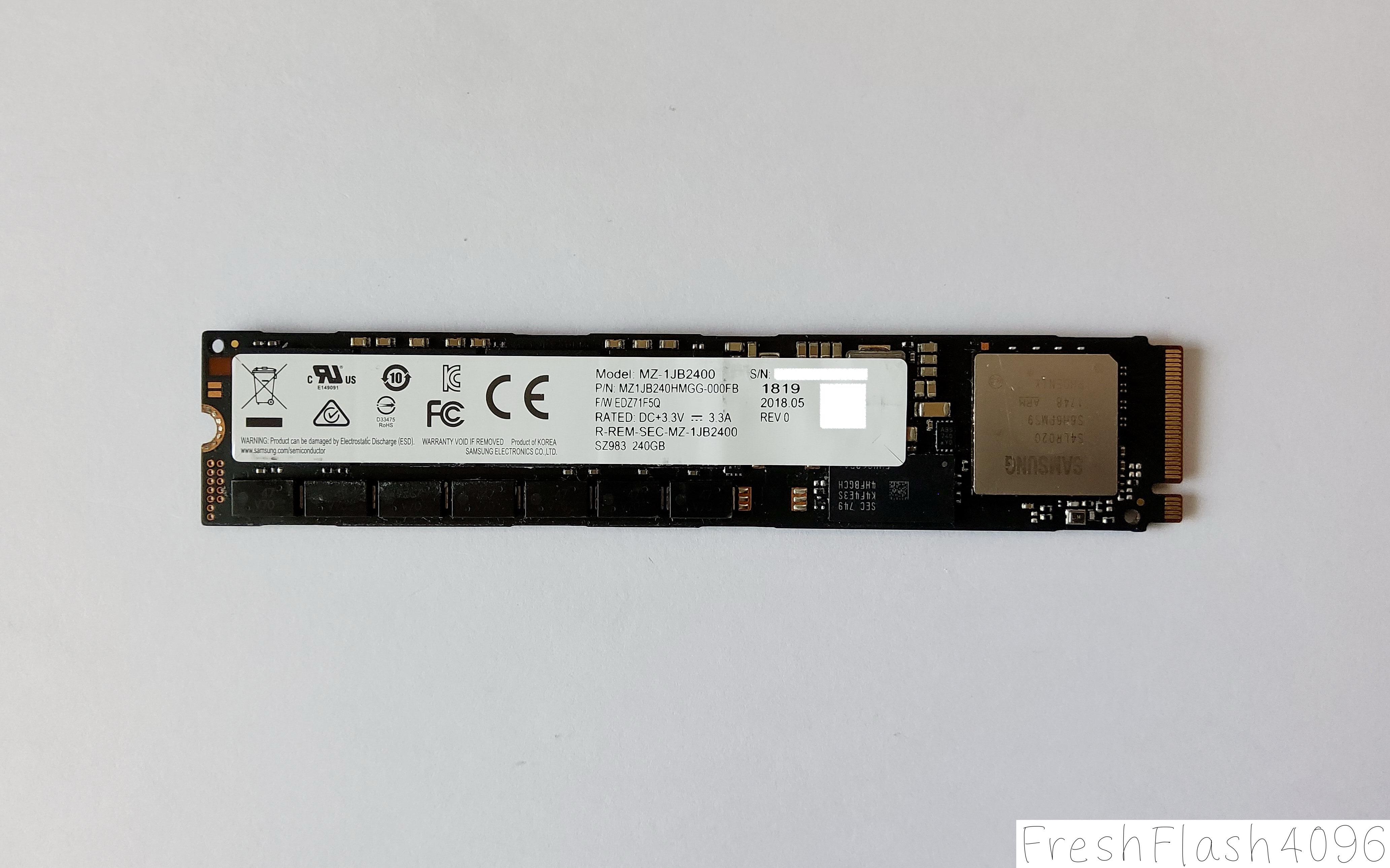
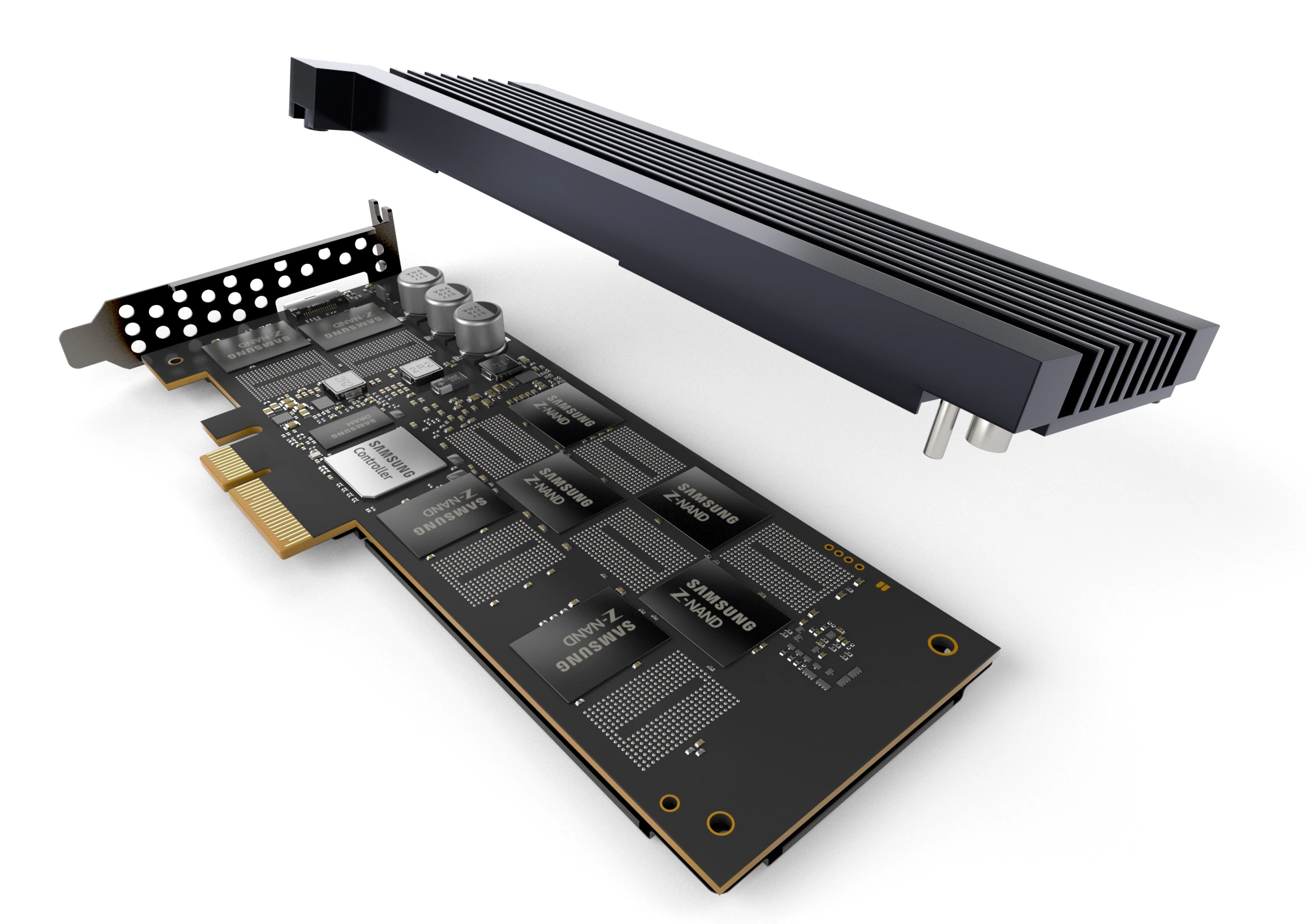
극저온 3D NAND 식각
Tokyo Electron(TEL)은 2023년 6월, IEEE Symposium on VLSI Technology & Circuits에서 Beyond 10um Depth Ultra-High Speed Etch Process with 84% Lower Carbon Footprint for Memory Channel Hole of 3D NAND Flash over 400 Layers를 발표했다.
해당 발표에선 극저온에서 높은 속도의 식각을 가지는 시스템을 구현했다. 아래에 논문의 Abstract를 인용한다.
A novel High-Aspect-Ratio (HAR) dielectric etch technology which is capable of etching beyond 10μm depth memory channel hole for future generations of 3D NAND flash memory has been successfully developed for the first time. Ten micron depth etching is not practical with conventional etching technology, but our novel technology using cryogenic wafer stage and new gas chemistry can achieve not only 10μm etch capability but also quite short process time (33 minutes) with 84% carbon footprint reduction of greenhouse gases. Etched profile was also confirmed to be excellent. Thus, this is a key technology for highly productive, cost effective and sustainable manufacturing of 3D NAND flash memory device.
400L 이상의 3D NAND에서 Single-Stack 또는 Double-Stack의 구축이 가능한 것으로도 기대되는데, 이러한 기술이 적용된 장비를 삼성에서는 직접 테스트하고 있으며, 하이닉스는 TEL에 웨이퍼를 보내 테스트를 진행하는 중이라 한다.
참고로 작년에 공개된 하이닉스의 321L 3D NAND는 Triple-Stack으로 구현되었으며, 삼성에서도 V10 이후부터는 Triple-Stack을 도입할 것이라 말한 적이 있다.
Comments